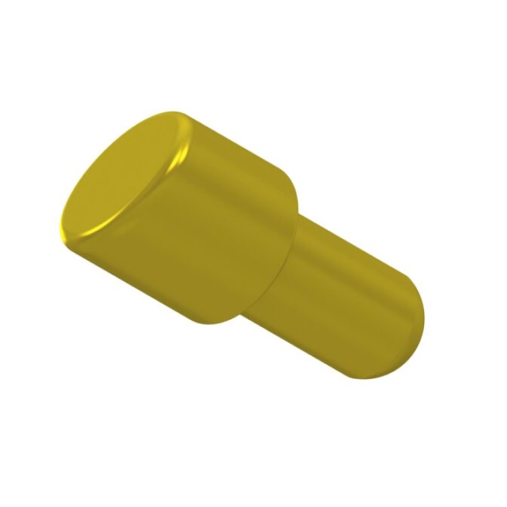
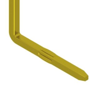
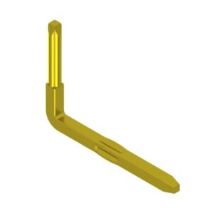
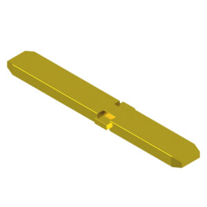
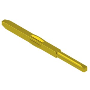
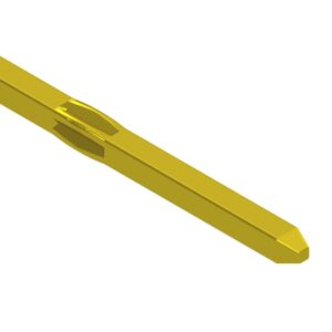
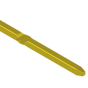
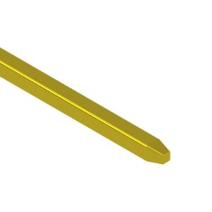
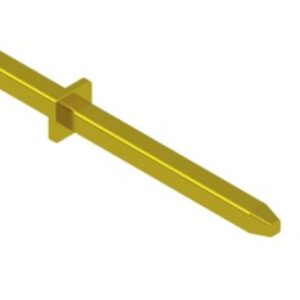
Plungers for Contact Probes


Our plunger products for probes are recommended for the following customers!
・Those who are promoting eco-friendly activities and are looking for an environmentally friendly plunger.
・Those who are having difficulty finding a plunger with the specifications they want.
・Those who are looking for a plunger with high conductivity or high thermal conductivity material.
・Those who want to eliminate probe sharp edges.
Main Applications
Semiconductor inspection equipment related
Inspection contact probe applications (spring probes, probe pins)
Contact probes for inspection measuring machines and inspection sockets for various electronic components, semiconductor devices, printed circuit boards, etc.
Consumer and industrial products
Spring connector applications (pogo pins)
Contact probes for inspection measuring machines and inspection sockets for smartphones, semiconductor devices, printed circuit boards, etc.
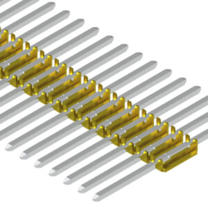
lineup
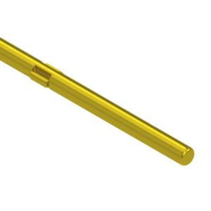
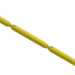
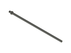
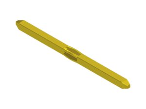
Machining Examples①
| Specifications | |
| Wire diameter | φ0.2mm~φ0.6mm |
| Total length | 5.0mm~10.0mm |
| Material | C2600 |
| C2700 | |
| C5191 | |
| Others | |
| Tip shape | Needle flat |
| Plating | Ni base + Au |
| Packing form | Bag |
| Case | |
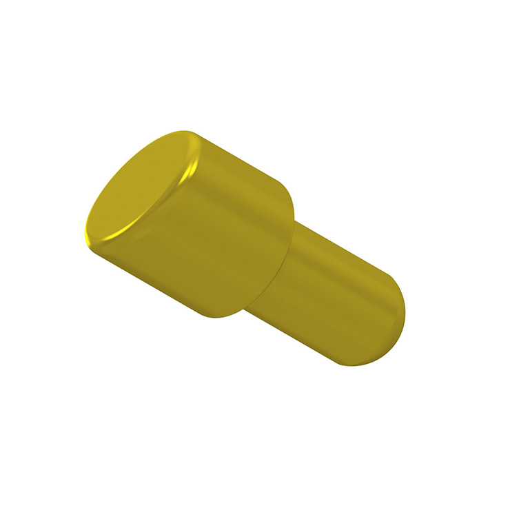
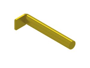
Machining Examples②
| Specifications | |
| Wire diameter | φ0.3mm~φ.8mm |
| Total length | 5.0mm~15.0mm |
| Material | C2600 |
| C2700 | |
| C5191 | |
| Others | |
| Tip shape | Flat |
| Round Flat | |
| Needle flat | |
| Concave | |
| Plating | Ni base + Au |
| Packing form | Bag |
| Case | |
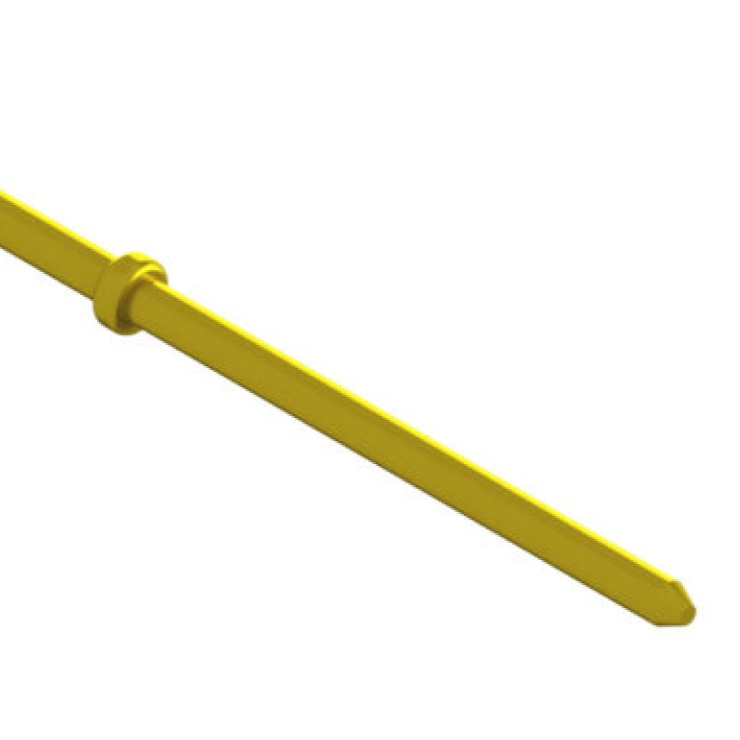
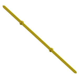
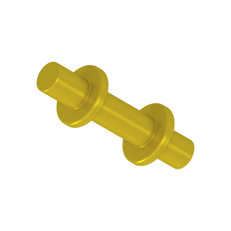
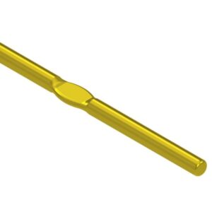
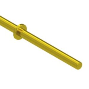
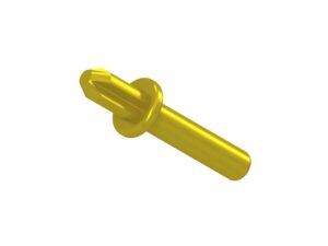
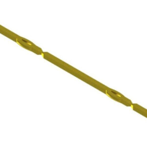
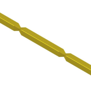
Machining Examples③

| Specifications | |
| Wire diameter | φ0.2mm~φ1.0mm |
| Total length | 5.0mm~10.0mm |
| Material | C2600 |
| C2700 | |
| C5191 | |
| Others | |
| Mid-flanged | Single |
| Double | |
| Tip shape | Flat |
| Plating | Ni base + Au |
| Packing form | Bag |
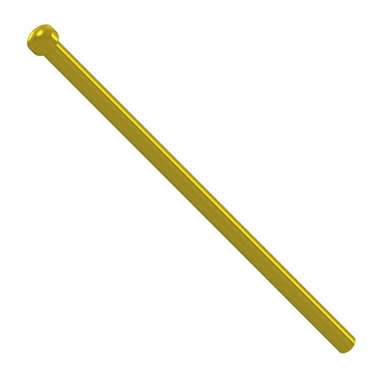
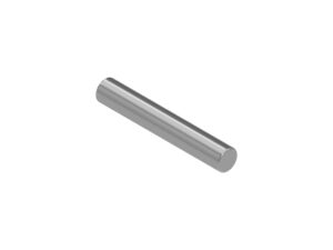
Machining Examples④
| Specifications | |
| Wire diameter | φ0.15mm~φ0.8mm |
| Total length | 0.5mm~3.0mm |
| Material | C2600 |
| C2700 | |
| C5191 | |
| Others | |
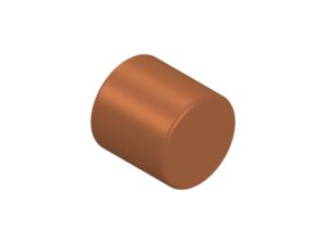
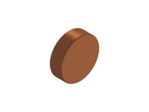
| Tip shape | Round |
| Plating | Ni base + Au |
| Packing form | Bag |
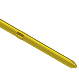
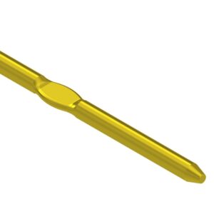
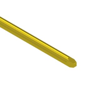
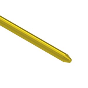
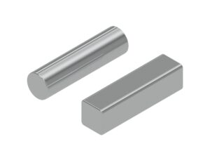
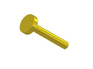
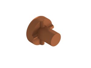
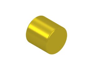
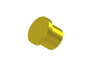
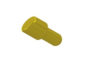
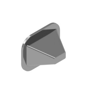
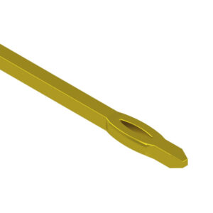
Tip Shape
| Shape | Round | Needle Flat | Concave | Flat |
| Figure | 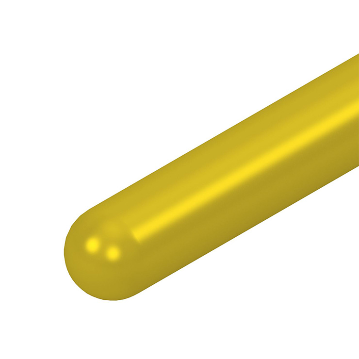 | 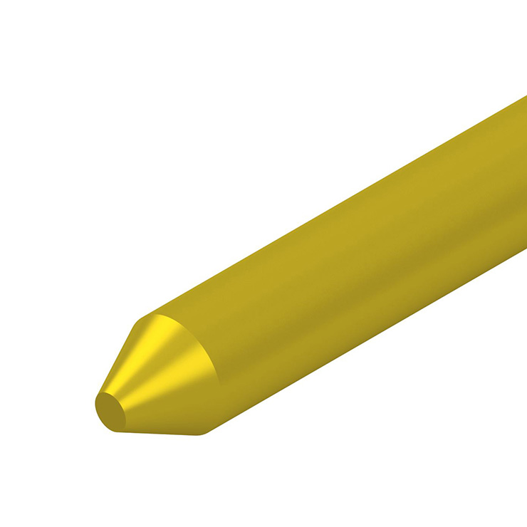 | 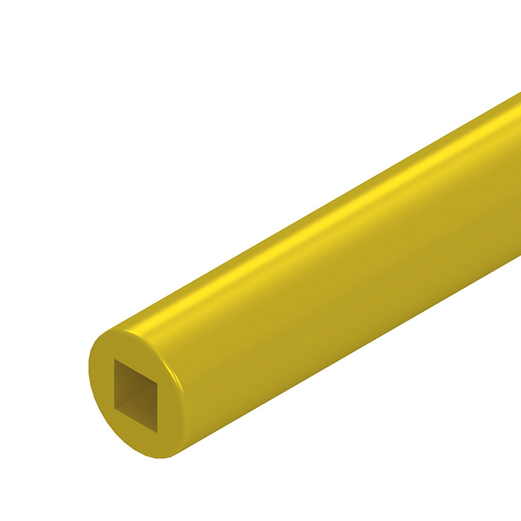 | |
| Features | Suitable for inspection with less damage to vulnerable contact surfaces. | Suitable for inspection of fine contact points due to the narrow tip. | Suitable for inspection by contact with solder balls. | Suitable for surface contact inspection. |
Material
Physical Properties
| component | C2600 | C2700 | C5191 | Highly conductive material |
| Specific gravity | 8.53 | 8.47 | 8.83 | Please inquire |
| thermal expansion coefficient[10-6/K] | 19.9 | 20.3 | 18.0 | |
| Thermal Conductivity[W/(m/K)] | 121 | 117 | 67 | |
| Conductivity[%IACS] | 28 | 27 | 14 | |
| Modulus of Longitudinal Elasticity[GPa] | 110 | 103 | 110 |
Chemical Properties
| component | C2600 | C2700 | C5191 | Highly conductive material |
| Cu[wt%] | 68.5~71.5 | 63.0~67.0 | Remaining portion | Please inquire |
| Pb[wt%] | ≦0.05 | ≦0.05 | ≦0.02 | |
| Fe[wt%] | ≦0.05 | ≦0.05 | ≦0.1 | |
| Zn[wt%] | Remaining portion | Remaining portion | ≦0.2 | |
| Sn[wt%] | - | - | 5.5~7.0 | |
| P[wt%] | - | - | 0.03~0.35 |
Features of our probe products
Cold forging process of wire rods allows the material to be used without wasting, which is eco-friendly because it does not generate chips due to cutting process.
To Cold forging process page >
Unique shape by forging process
Advantages and disadvantages of cold forging >
Related Links
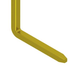
Products with the Same Shape
-
Embossed Taping (terminal pins & tiny components) -
Mid-flanged straight pins with conical tapers -
Straight pins with conical tapers and cross-shaped cross sections -
Partially pinched straight pins with conical tapers -
Partially flattened straight pins with conical tapers -
Straight pins with 4-side tapers from round wires -
Straight pins with conical tapers from round wires -
Partially flattened straight pins with round chamfers -
Partially pinched straight pins with round chamfers -
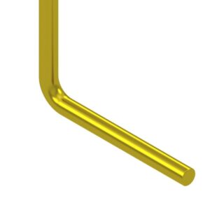
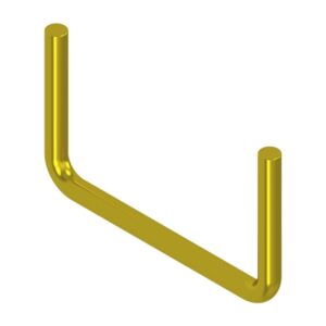
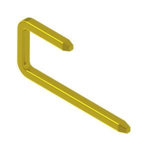
L-shaped pins (right angle) -
Double-step L-shaped pins -
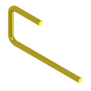
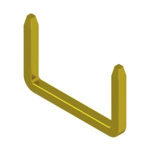
U-shaped pins -
J-shaped round pins -
Partially flattened L-shaped pins -
High-volume Pins -
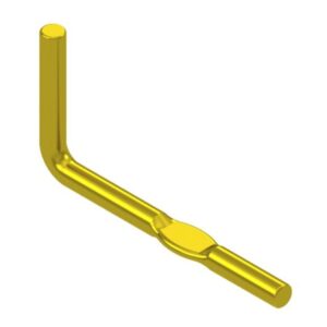
Mid-flanged straight pins with round chamfers -
Bandolier terminals / pins made from round wires -
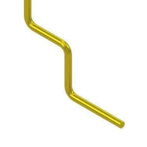
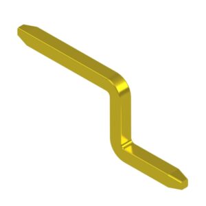
Crank shaped pins -
End-to-end pins / End-to-end terminals (round type) -
Block terminals (heat dissipation terminals and block pins) -
Connector Assembly with Wire Terminals -
Surface Treatment (Plating) -
Terminals with solder -
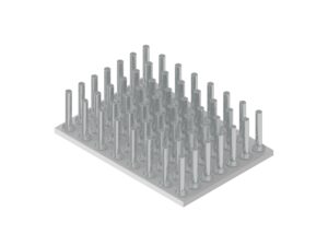
Heat radiating pins for heat sinks -
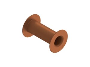
Rivet (Pin holder, Terminal holder) -
PGA Pins (Terminals for CPUs) -

Lead pins / Diode terminals -

Jumper pins -
Press-fit terminals (from wire) -

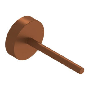
Substrate terminals / Post pins -
Antenna Pins -
Quartz resonator terminals (hermetic seal terminals) -
Conductive terminals -
Kovar pins (electrode pins) -
Leadless diode terminals / Dumet pins -
Brazing filler metal cut pieces (gold, silver, copper, etc.) -
Ultra-small pins, extra-fine pins, micro pins -
Plungers for Contact Probes -
Copper Pillar pin -
Copper inlay
Products with the Same Processing Method
-
Embossed Taping (terminal pins & tiny components) -
Press-fit bandolier terminals -
Deep drawn pins / cups -
Pyramidal pins -
U-shaped pins Pyramidal pins -
Crank-shaped pins Pyramidal pins -
J-shaped square pins -
L-shaped pins Pyramidal pins and cross-shaped cross sections -
Swaged L-shaped pins Pyramidal pins and cross-shaped cross sections -
„ear-crush“ flat square with pyramid taper -
Swaged straight pins Pyramidal pins and cross-shaped cross sections -
Straight pins Pyramidal pins and cross-shaped cross sections -

Partially pinched straight pins Pyramidal pins -
Partially flattened straight pins Pyramidal pins -
Straight pins Pyramidal pins -
Mid-flanged straight pins with conical tapers -
Straight pins with conical tapers and cross-shaped cross sections -
Partially pinched straight pins with conical tapers -
Partially flattened straight pins with conical tapers -
Straight pins with 4-side tapers from round wires -
Straight pins with conical tapers from round wires -
Partially flattened straight pins with round chamfers -
Partially pinched straight pins with round chamfers -
L-shaped pins (right angle) -
Double-step L-shaped pins -
U-shaped pins -
J-shaped round pins -
Partially flattened L-shaped pins -
High-volume Pins -
L-shaped pins Pyramidal pins -
Mid-flanged straight pins Pyramidal pins -
Mid-flanged straight pins with round chamfers -
Needle-eye square press-fit -
Bandolier terminals / pins made from square or flat square wires -
Bandolier terminals / pins made from round wires -
Crank shaped pins -
End-to-end pins / End-to-end terminals (press-fit type) -
End-to-end pins / End-to-end terminals (square type) -
End-to-end pins / End-to-end terminals (round type) -
Block terminals (heat dissipation terminals and block pins) -
Terminals with solder -
Heat radiating pins for heat sinks -
Rivet (Pin holder, Terminal holder) -
Hollow Rivet -
PGA Pins (Terminals for CPUs) -
Connector terminals / Connector pins -
Lead pins / Diode terminals -
Jumper pins -
Press-fit terminals (from wire) -
Substrate terminals / Post pins -
Antenna Pins -
Quartz resonator terminals (hermetic seal terminals) -
Conductive terminals -
Kovar pins (electrode pins) -
Leadless diode terminals / Dumet pins -
Brazing filler metal cut pieces (gold, silver, copper, etc.) -
Ultra-small pins, extra-fine pins, micro pins -
Plungers for Contact Probes -
Copper Pillar pin -
Copper inlay -
Electrode Terminals of Rechargeable Battery